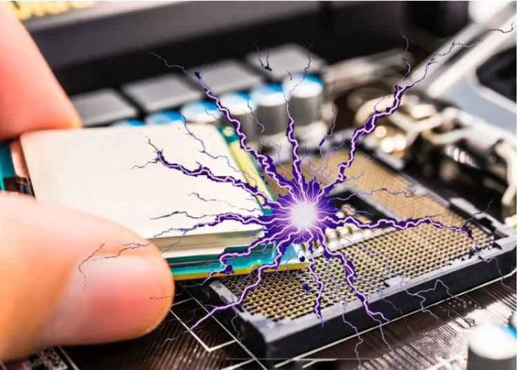
In contemporary electronics manufacturing, electrostatic discharge (ESD) represents a pervasive and costly threat to sensitive components. Even minor static sparks as low as 100 volts can irreparably damage integrated circuits, leading to latent failures or immediate malfunction. ESD packaging employs scientifically engineered solutions to mitigate these risks through multiple physical principles and material innovations.
- Static-Dissipative Materials
ESD packaging utilizes polymers with precisely controlled surface resistance ranging from 10⁶ to 10⁹ ohms per square meter. These materials (e.g., polyethylene embedded with carbon nanoparticles) create a controlled conductive pathway. This allows accumulated electrostatic charges to dissipate gradually to ground within milliseconds, preventing sudden discharges. Standard insulating plastics exceed 10¹² Ω/m², enabling dangerous charge accumulation, while highly conductive materials (<10⁵ Ω/m²) risk creating rapid discharge events.
- Faraday Cage Shielding Mechanism
Metallized shielding bags constructed from aluminum-coated PET laminates form continuous conductive enclosures. According to electromagnetic theory, when external electrostatic fields interact with such packaging, mobile electrons redistribute across the outer surface, generating counteracting fields that neutralize internal electric fields. Laboratory testing confirms these structures effectively block ESD events up to 30,000 volts, creating a “quiet zone” for components.
- Triboelectric Charge Suppression
Internal packaging layers incorporate ionic antistatic agents (e.g., quaternary ammonium compounds) that migrate to the surface. These hygroscopic substances absorb atmospheric moisture, forming a microscopic conductive water layer. This layer reduces friction coefficient during component movement and limits triboelectric charge generation to below 10 nanocoulombs per square centimeter – significantly under the 50 nC/cm² threshold known to trigger arc discharges.
- Multi-Layer Structural Defense
High-performance packaging employs stratified architectures:
– Outer shell: 75μm biaxially-oriented PET film provides mechanical rigidity and abrasion resistance
– Intermediate barrier: 12μm aluminum foil reflects electromagnetic interference and creates moisture barrier
– Inner liner: Conductive polyurethane foam (surface resistivity 10⁸ Ω) with cushioning properties
Transport simulation tests demonstrate 98% reduction in component damage under ISTA 3A vibration profiles.
- Environmental Adaptation Systems
Advanced packaging integrates humidity-responsive materials such as lithium chloride-doped polymers. These “smart” materials automatically increase ionic conductivity when ambient relative humidity drops below 40%. Surface resistance dynamically decreases from 10¹⁰ Ω at 30% RH to 10⁸ Ω at 60% RH, maintaining consistent ESD protection across global climatic zones from arid deserts to tropical regions.
Industry Validation & Standards Compliance
According to ESD Association data, compliant packaging reduces ESD-related production losses from 9.2% to under 0.5%. As semiconductor geometries shrink below 5nm (with ESD sensitivity thresholds approaching 10 volts), adherence to ANSI/ESD S20.20 and IEC 61340-5-1 standards becomes critical. Modern packaging undergoes rigorous qualification including:
– Surface resistance mapping with concentric ring probes per ESD STM11.11
– Charge decay testing per ESD STM11.31
– Shielding effectiveness verification per MIL-STD-1686
Leading manufacturers now embed RFID-enabled sensors that continuously monitor:
– Real-time static charge accumulation
– Environmental humidity exposure
– Shock/vibration events during transit
This data transmits to cloud platforms via 5G-enabled logistics hubs, enabling predictive protection throughout supply chains.
Economic Impact & Future Trends
The global ESD packaging market is projected to reach $6.2 billion by 2028 (CAGR 5.7%), driven by IoT proliferation and 5G infrastructure deployment. Emerging technologies include:
– Self-healing conductive polymers with carbon nanotube networks
– Biodegradable antistatic composites from cellulose nanofibers
– Quantum tunneling composites (QTCs) that switch from insulating to conductive states under pressure
As electronic components continue miniaturizing, ESD packaging remains the indispensable guardian against invisible electrostatic threats, preserving trillions of dollars in global electronics commerce annually.