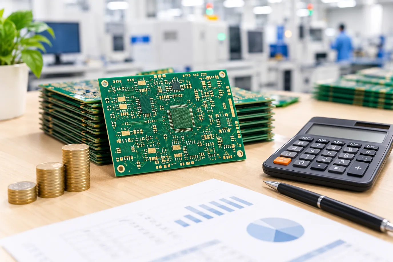
A custom PCB can cost less than one dollar per board or several hundred dollars per board. The difference is not simply the board’s dimensions. Layer count, laminate, copper weight, hole structure, surface finish, production volume, testing, and lead time all influence the quotation.
Two boards with the same outline may therefore have completely different prices. One might use standard two-layer FR-4 and through-holes, while the other requires controlled impedance, heavy copper, blind vias, and ENIG.
Understanding how manufacturers calculate these costs makes it easier to set a realistic budget and identify design changes that deliver genuine savings.
How Much Does a Custom PCB Cost?
Public prices from online PCB manufacturers provide a useful starting point. The figures below were checked in September 2026.
| PCB category | Publicly advertised starting price | Typical entry-level order |
|---|---|---|
| Standard FR-4 PCB | 5-10 prototype boards | |
| Aluminum or metal-core PCB | 5 boards | |
| Flexible or rigid-flex PCB | About | Small prototype order |
| High-frequency or Rogers PCB | About | 5 prototype boards |
| HDI PCB | About | Small prototype order |
| Basic PCB assembly service | From | Assembly service only; parts and fabrication may be separate |
These are promotional starting prices, not guaranteed quotations. They normally assume small dimensions, standard specifications, common materials, generous manufacturing rules, and a standard lead time.
Shipping, taxes, components, tooling, special testing, engineering review, and advanced options may not be included. A five-board order advertised at $5 can easily have a delivered cost of $30 or more after freight and optional services are added.
The figures are still useful because they show the scale of the difference between standard FR-4 production and specialized technologies such as HDI, rigid-flex, and high-frequency fabrication.
Board Area Is Only Part of the Calculation
PCBs are manufactured on production panels rather than processed individually. Several copies of a board are arranged on a larger panel and pass through imaging, etching, drilling, plating, solder-mask application, and inspection together.
The manufacturer is therefore interested in how efficiently the design fits on its standard panel.
A small dimensional change may allow another row of boards to fit. An irregular outline, excessive breakaway area, or inconvenient dimension may leave material unused. As a result, a slightly larger rectangular board can sometimes cost less than a smaller board with an inefficient shape.
When requesting a Custom PCB Manufacturing quote, ask whether adjusting the outline, delivery panel, or breakaway rails could improve panel utilization.
Prototype suppliers may also combine compatible orders from different customers on the same production panel. This process, commonly called order pooling, helps distribute setup and material costs. A design using an uncommon laminate, copper weight, or finish may not qualify for the same savings.
How Specifications Affect the Price
The table below shows how common design decisions influence manufacturing cost.
| Design decision | Lower-cost option | Higher-cost option | Why the price changes |
|---|---|---|---|
| Layer count | 1-2 layers | 6, 8, 12, or more layers | More material, imaging, alignment, lamination, and inspection |
| Material | Standard FR-4 | Rogers, PTFE, polyimide, ceramic, or metal core | Specialized materials cost more and may require separate processing |
| Copper weight | 1 oz | 2-4 oz or heavier | More copper is used and fine etching becomes harder |
| Via structure | Standard through-hole vias | Blind, buried, microvia, or via-in-pad | Extra drilling, filling, planarization, or lamination may be required |
| Trace and spacing | Standard production rules | Very fine lines and clearances | Tighter controls can reduce manufacturing yield |
| Surface finish | HASL or OSP | ENIG, ENEPIG, hard gold, or other specialist finishes | Additional materials and process stages are required |
| Testing | Standard electrical test | Impedance, microsection, X-ray, or functional testing | More equipment and inspection time are needed |
| Lead time | Standard production | 24- or 48-hour rush service | The order requires priority scheduling and dedicated capacity |
| Quantity | Production batch | Very small prototype order | Fixed setup expenses are divided among fewer boards |
The cost effect is cumulative. A six-layer board with ordinary through-holes may remain relatively affordable. A six-layer board that also requires laser microvias, high-frequency laminate, 3 oz copper, and ENEPIG will belong to a very different price category.
Layer Count and Stack-Up
Adding layers does more than add copper sheets. A multilayer PCB requires additional cores and prepreg, inner-layer imaging, alignment, lamination, drilling, and inspection.
Controlled-impedance boards may also need specific dielectric thicknesses and copper weights. This limits the manufacturer’s ability to substitute stocked materials or use a standard stack-up.
Additional layers may still reduce the total product cost if they allow a smaller board, improve electromagnetic compatibility, or prevent signal-integrity failures. The objective should be to use the simplest stack-up that reliably meets the electrical requirements.
For early budgeting, buyers should expect a four-layer board to cost more than a standard two-layer board, while six-layer and higher designs move progressively further away from promotional prototype pricing.
Material and Copper Selection
Standard FR-4 is usually the most economical material because it is widely stocked and processed in large volumes. Costs increase when the design requires:
- High-Tg laminate
- Low-loss RF or microwave material
- Flexible polyimide
- Aluminum or copper core
- Ceramic substrate
- Halogen-free material
- Heavy copper
- A specific branded laminate
Material availability matters as much as the material price. A special laminate that is not in stock may create a minimum purchase requirement and extend the lead time.
Where the application permits it, defining the required electrical and thermal properties while allowing an approved equivalent material can create more sourcing flexibility.
Thicker copper also affects the etching process. Maintaining fine traces and spacing becomes more difficult as copper thickness increases. Combining heavy copper with dense routing can therefore add more cost than either requirement would create by itself.
Trace Width, Hole Size, and Advanced Vias
Every PCB manufacturer has a standard process window. Designs that remain comfortably within it are easier to produce at a high yield.
Prices can rise when a design includes:
- Very narrow traces or spacing
- Extremely small drilled holes
- High drill aspect ratios
- Tight annular rings
- Blind or buried vias
- Laser-drilled microvias
- Stacked microvias
- Filled and plated-over vias
- Back drilling
- Tight registration tolerances
A standard through-hole via generally passes through the board in one drilling and plating sequence. Blind, buried, and stacked structures may require additional drilling or sequential lamination cycles.
Via-in-pad can be valuable beneath BGAs, but filling and planarization add processing stages. It should be used because the layout needs it, not simply as a default routing preference.
Choosing a Surface Finish
HASL is commonly among the lower-cost surface finishes and works well for many conventional products. OSP can also be economical, although its storage and handling requirements should be considered.
ENIG costs more but provides a flat surface suitable for fine-pitch components and exposed pads. Hard gold, ENEPIG, immersion silver, and immersion tin serve more specialized applications and can increase the quotation further.
The cheapest finish is not always the least expensive choice overall. A finish that creates soldering difficulties, contact wear, or shelf-life problems can produce much higher assembly and warranty costs.
The selection should be based on component pitch, storage time, assembly cycles, contact requirements, environmental compliance, and the expected operating environment.
Compare Landed Cost Instead of the Headline Price
A $5 fabrication offer is not a $5 delivered order. The complete purchasing calculation should include:
Landed cost per usable board = fabrication + setup + testing + freight + duties + expected rework, divided by the number of accepted boards
When assessing a supplier such as OrinewPCB, provide a complete manufacturing package and ask the supplier to identify every feature that falls outside its standard process. This helps determine whether the initial price reflects the real design or only a basic estimate based on dimensions and quantity.
Buyers should compare the following items across quotations:
- Fabrication price
- Tooling and setup
- Electrical testing
- Engineering review
- Delivery-panel charges
- Packaging
- Freight and taxes
- Lead time
- Quality documentation
- Replacement terms
- Engineering support
A manufacturer that identifies an unnecessary microvia, unsuitable finish, or inefficient panel arrangement before production may save more than a supplier offering a slightly lower headline price.
Final Thoughts
Standard FR-4 prototypes may begin at only $2-$5 for a small batch, but this figure represents the simplest end of the market. Flexible, high-frequency, rigid-flex, and HDI designs can begin at tens or hundreds of dollars before shipping and optional services.
The final price is determined by the manufacturing route, not just the board outline. Panel utilization, layer structure, laminate, copper weight, feature size, via technology, finish, testing, quantity, and lead time all matter.
The most effective savings usually happen before production. Using standard materials, keeping design rules within a proven process window, choosing advanced features selectively, and requesting early DFM feedback can reduce both the quoted price and the risk of defects.
Instead of asking only which supplier has the lowest price per board, ask which combination of design and manufacturing process delivers the lowest cost per reliable, usable board.